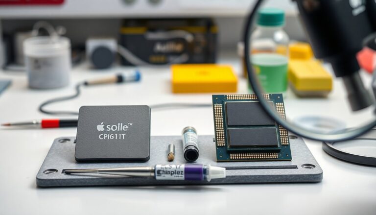
Apple is reportedly moving to a modular M5 family built from tightly connected chiplets, using TSMC’s SoIC advanced packaging. Instead of one large, monolithic die, future M5 Pro and M5 Max chips would pair separate CPU and GPU tiles inside a single package — a shift that could reshape Apple’s laptop silicon strategy and the broader ARM laptop market.
Why modular SoCs now
Apple’s tilt toward chiplets reflects practical pressures: shrinking node economics, thermal realities and the need for faster product iteration. By breaking a SoC into smaller tiles, Apple can isolate the most advanced CPU logic from larger I/O, analog or GPU blocks. That improves effective yields, simplifies tiered SKUs and gives engineers more flexibility to upgrade individual components without redoing a massive reticle. In plain terms: fewer costly wafers ruined by a single defect, and clearer, faster paths for incremental improvements.
What SoIC brings — and what it demands
TSMC’s SoIC lets die sit closer together with very high-bandwidth, low-latency links. That preserves much of the performance density of a single die while unlocking modularity. But the benefits come with new headaches. Vertical stacking concentrates heat in tighter volumes, so cooling designs that worked for monolithic chips won’t always translate directly. Inter-die fabrics consume power, add design complexity, and require rigorous verification to ensure coherence, low latency and reliability across tiles.
From my time at Deutsche Bank, the trade-off looks familiar: you move risk out of one gigantic asset and spread it across smaller, more manageable pieces. That can make operations more resilient and upgradeable — but it also creates new integration costs and governance requirements. Packaging partners, substrate suppliers and OS vendors must coordinate closely; firmware and drivers need to treat the chiplet ensemble as a tightly coupled system, not a single silicon block.
Thermals, power and validation
Separating CPU and GPU into distinct tiles eases SKU differentiation but tightens the requirements for power delivery, clock domains and memory consistency. Engineers will need to refine voltage islands, power-state transitions, and system-level orchestration to get the promised efficiency gains. On the manufacturing side, tile-level testing allows salvage of good blocks into mixed assemblies, but multi-die packages demand more sophisticated burn-in and thermal cycling at the package level, increasing OSAT throughput needs and potentially lengthening lead times.
Stacked dies shorten interconnects and boost bandwidth, yet they also raise thermal density. Sustained workloads that push packages toward 80–100W or beyond put a spotlight on cooling solutions: thicker heat spreaders, enhanced heat pipes, or different chassis trade-offs that affect weight, cost and acoustics. From a compliance perspective, these design shifts can affect supplier due diligence and regulatory checks tied to thermal safety and export controls.
Market and competitive implications
If Apple pulls this off without sacrificing performance-per-watt, it will raise the bar for rivals. Competitors must match inter-tile bandwidth while keeping energy overhead low, and prove system-level reliability and thermal safety to satisfy OEMs and regulators. Qualcomm, which has favored more monolithic laptop ARM designs to date, faces a choice: continue optimizing single-die approaches or invest heavily in advanced packaging and co-design with OEMs.
A switch to chiplets is not just an engineering decision but a commercial one. It involves capital for packaging R&D, revamped supply-chain relationships, and closer collaboration across firmware, OS, and mechanical teams. For some vendors, the path will be long and costly; for others, chiplets could unlock better yields and faster refresh cycles that translate into market wins.
Signals to watch
Early indicators will make the picture clearer: supplier confirmations, first device teardowns showing SoIC-style stacked dies, independent sustained-performance benchmarks, and commentary from foundries and OSATs. Also pay attention to OEM thermal briefs, Qualcomm’s partner agreements and R&D spend on interposers and substrates. Those clues will tell us whether chiplets become the dominant route or remain one of several viable architectures. The approach promises yield gains and faster SKU scaling, but it requires solving tougher problems around heat, power delivery, validation and supply-chain coordination. Execution will determine whether this is a genuine step-change for mobile silicon — or a complex trade that only the best-resourced teams can pull off.

